
X-Ray Imaging and Non-Destructive Testing
 X-ray imaging is a direct non-destructive testing (NDT) method which can be applied to a wide range products and devices manufactured in many industry sectors. It can photographically investigate any object whether at the surface or buried within a block of material. The technique is a very versatile so it can be used to evaluate products and devices where components are manufactured from different materials and can be combined with other techniques such as optical microscopy and SEM/EDX together with reverse engineering techniques like cross-sectioning to determine the root cause of failures or target specific areas for chemical analysis.
Typical Applications of X-ray Imaging
- Medical device monitoring of stents, MDI components, metal debris in polymer components and wound management systems.
- Automotive and aerospace components inspection like electrical coils and turbine blades.
- Packaging applications like food cans, blister packaging contents and metallic debris.
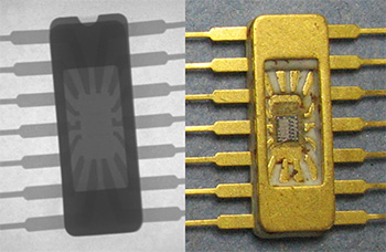
- Microelectronics inspection looking for physical failures in chip packaging, encapsulation or wire bonding failures. The X-ray image below shows the fine gold wire bonds but the failure appears associated with an uneven level of central chip adhesive.
- Power Electronics examination including failure in potted power electronic units.
- Metallurgy including failure investigation of engine components and suitability of manufactured articles like engine part comparisons.
- Non-destructive testing looking for cracks and voids in materials, metals, welds and joints.
Principles of X-ray Imaging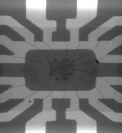
X-ray imaging produces a cumulative absorption map or photo, so that the image presents a summation of the layers of material within a sample. During X-ray imaging, a micro-focussed X-ray source irradiates the samples on a X-Y movable sample stage, and the unabsorbed X-rays are collected by a variable magnification detector. X-ray voltage and current can be adjusted, along with image brightness and contrast. An X-ray image of a typical component provides information on its structure where the mean atomic number influences the X-ray image contrast.
Sample Analysis Capabilities and Limits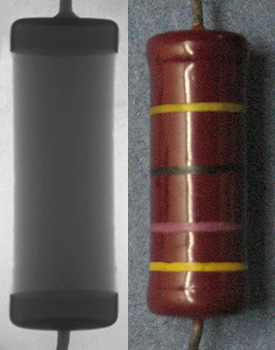
The X-ray imaging system can inspect sample who's lateral dimensions are from a few mm up to approximately 600mm. The sample thickness can be up to 100-200mm, but the exact upper limit is dependent on the atomic number contrast, as smaller differences in density and atomic numbers of component materials are more difficult to resolve in a thicker samples.
For an individual image the individual map field of view is between 5x5mm and 60x60mm. The smallest resolvable feature is around 5um with a maximum magnification of approximately 1000x. Limits ultimately depend on the level of contrast (ie atomic number difference) between the feature of interest and the surrounding materials.