
Electronic Devices and PCB Failure Investigations
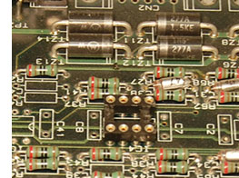
Microelectronics forms an integral part of a large proportion of products to control or monitor operation of mechanical parts and sensors or, in the case of consumer electronics, is the heart of the product itself. Printed Circuit Boards PCB’s are often now commonly manufactured abroad under contract for cost-reduction from suppliers and the supply chains need careful quality management control. It can be difficult to determine the root cause and where the manufacturing issues occur especially when there can be multiple suppliers in differing countries, with differing standards of quality control and reliability. It’s possible a supplier will not acknowledge whether they have an issue, and due to its presence in the supply chain, teasing out the process variation or issue can be difficult and time consuming. The rapid determination of failures on finished product is essential to prevent ‘bad’ inventory build-up, correct process variation, prevent waste and prevent customer returns.
Examples of PCB microelectronics and driver electronics component process problems the laboratory has worked on include:-
 Engine management systems.
- Staining and shorting from resin flux residues proved by FTIR
- PCB ionic contamination measurements
- PCB non-ionic contamination investigations
- Mobile and commercial communications devices.
- Battery, power packs and transformer charging systems.
- Ribbon cable and interconnect failures from poorly controlled metal deposition and cleaning processes.
- Delaminating, conformal coating variation, and protective coating failures giving peeling and de-wetting.
- Corrosion or service life issues from flux residues.
- Attack of silver switch contactors by sulphur compounds giving high resistance.
- Physical and electrical gas or electrical sensor errors.
- Docking station; pin contamination and cleaning recommendations.
- Identification of incorrect solder alloy types, as required by RoHS for solder containing banned lead.
- Residual flux from soldering giving corrosion problems in moist application atmospheres. Detection of chlorine corrosion accelerant indicating perhaps a chlorinated flux which can corrode components.
- Incomplete solder reflow or wave soldering due to contamination issues.
- Wire bonding interfacial failures.
- Flaking or delaminating gold contact pads from poorly controlled electroless metal deposition baths.
- Switch or button pad failures generated by corrosion and poor PCB packaging practices.
- Inductor insulation cracking and delamination failures.
- Incompatibility of encasements with sensors and electronics.
- Failing relays on PCB after shipping.
- Degraded contact metallisation and discolouration of electronic housing in sealed control units.
- Lead presence in re-worked PCBs from lead-free process.
- Root-cause of PCB failure when control unit caught fire.
- Defects within solder balls, solder splashes, swarf from cutting, flux residues.
- Confirmation of the materials used in the circuit board – plating layers, solder types.
- Cross-section of circuit boards to look for cracks in solder areas.
- Potential sources of failure fire and analysis of nearby circuitry areas and/or good and bad boards to indicate reasons for fire.
- Checking solder for banned/illegal chemicals like Lead in solder for personal use products like e-cigarettes.
- Investigation of electrical cable construction.
- Detection of zinc whiskers in data centres using SEM / EDX.
- Delamination of glass and coatings in solar cells by XPS and SEM / EDX
Our laboratory analysts have considerable technical expertise in solving process, production, yield, and customer return issues in electrical and electronic devices, PCB boards and assemblies, soldering and solder pastes plus microelectronics.
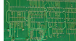
Printed circuit boards, electronic components, switches, relays and sensors, completed devices and their interconnections can all suffer process variation and in the worst case, failures either during manufacture, assembly, at the end of line or out in the field. Purity of chemicals and materials baths as well as maintenance of procedures are essential in such assembly lines to keep high quality output as per their customer's specifications. Deviation from procedure or over use of cleaning baths etc. not apparent at earlier inspection stages can result in low yield and customer rejects. Defects, residues and contaminants are frequently solved using optical microscopy, SEM / EDX, FTIR and IC methods.
The laboratory has performed many root cause investigations following electrical and electronic testing of the fault by the customer. Simply identifying where the electrical fault lies in a product does not indicate where or how the process root cause has occurred or the physical nature of the fault that could give rise to those electrical characteristics (as required by an 8D methodology). Physical Failure Analysis and Reverse Engineering can be used to reveal possible causes, where in the process the fault likely occurred and how. From this targeting, the laboratory can offer practical solutions and recommendations to change process and product quality procedures, to generate containment actions or more permanent preventative measures.
Typical problems the laboratory has investigated on behalf of its clients are to determine the physical reason for electrical faults such as shorts, open circuits or intermittent faults. The methodology of the laboratory is often to look at a known ‘good’-‘bad’ paired comparison with electrical signatures and characterisation to identify the physical fault. From this simple method, the important layer or levels the fault occurred at and relevancy to the failure are quickly established. Knowing the processing and materials present, reverse engineering can be undertaken to identify exactly where the process is out of control and recommend ways in which the problem could be tested, improved, controlled or fixed.
The laboratory's primary contacts for these sorts of issues is Dr Simon Romani and Howard Coulson.